Die Attach
Die Attach Techniques
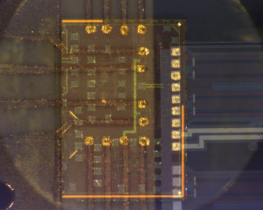
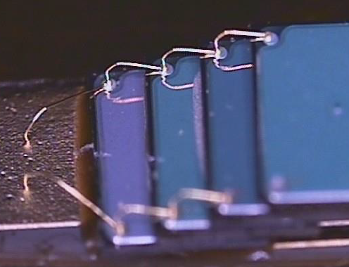
Die attach or die bonding is the process of attaching a semiconductor die to a package, a substrate such as a PCB board or another die. The die attach process is fundamental to multiple types of packaging.
Examples
Die Attach Processes
The four common types of die attach processes offer differing bond properties and use either distinct workflow procedures or different materials.
Adhesive BondingAdhesive die attach makes use of adhesives such as epoxy and polyimide to form a bond between a die and a package/substrate/another die. | |
Eutectic BondingEutectic bonding refers to attaching a die to a package or a substrate using a metal alloy as an intermediate layer to form a continuous bond. A eutectic bond is formed when the metal alloy in the melted state forms atomic contact with the die and the substrate. | 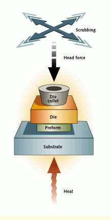 |
Solder AttachDie is attached using a solder/solder paste. | 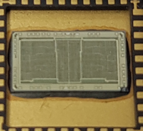 |
Flip ChipFlip chip is a die attach method where the electrical connections between the chip and package/substrate are made directly by inverting the die face-down onto the substrate/package. | 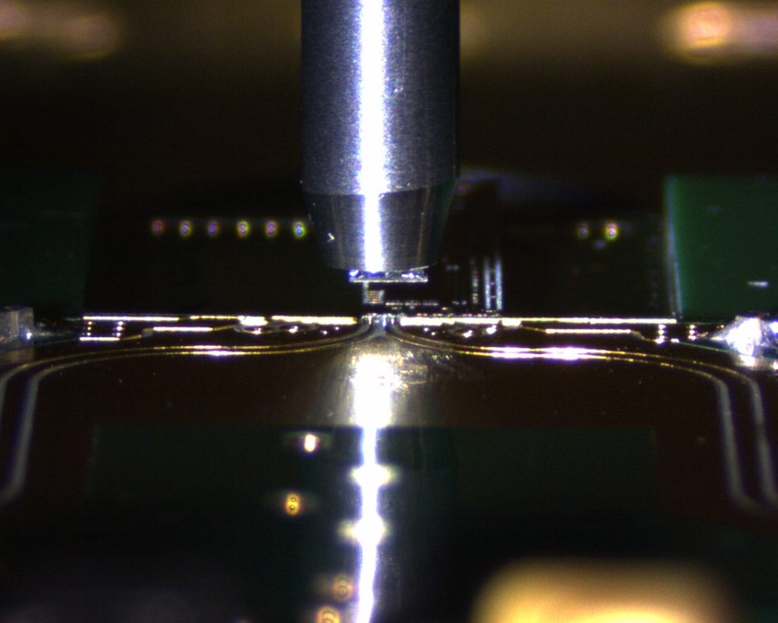 |
Additional Information
Die bonding processes are application specific where the operating conditions, environment and reliability requirements for the electronic device are considered. Forming a bond/joint between the die and the package, substrate or another die and its precise placement is a multifunctional process which aims to achieve the following:
- Mechanically fix the die onto the package, substrate or another die.
- Create a uniform contact between the die and other surfaces.
- Good heat dissipation for the die and to withstand temperature extremes without degrading.
- High thermal stability to reduce temperature induced mechanical stress in the bond/joint between the die and the package, substrate or another die.
General Die Attach Work Flow
Bonding Material Selection
A bonding material such as adhesive, eutectic preform or solder paste is deposited on a specific area of the substrate/package. The bonding material may be dispensed or dip coated on a substrate/package. In case of flip chip, gold balls/bumps are deposited first on the die.
Die Attach at our Facility |