Welcome!
Welcome to our website dedicated to electronic and optical device packaging. We hope you find the information you need about the processes involved in semiconductor packaging, examples of our work and the tools and techniques used at our facility. If you cannot find the information you need please do make contact with us.
Wire Bonding
Electrical interconnections are made between the die and the driver components.
Encapsulation
The die and its electrical interconnections are protected from their environment by a physical barrier.
Quality
The strength of die and wire bonds, the validity of encapsulation and the overall reliability of the packaged die is quantitatively and qualitatively analysed.
Typical Process |
Types of Packaging
Traditional Package AssemblyThe die is placed in a die package traditionally consisting of metal, ceramic or plastic casing depending on the application. Package choice depends on issues such as the necessary heat dissipation, cost, reliability and operating environmental conditions of the device. | 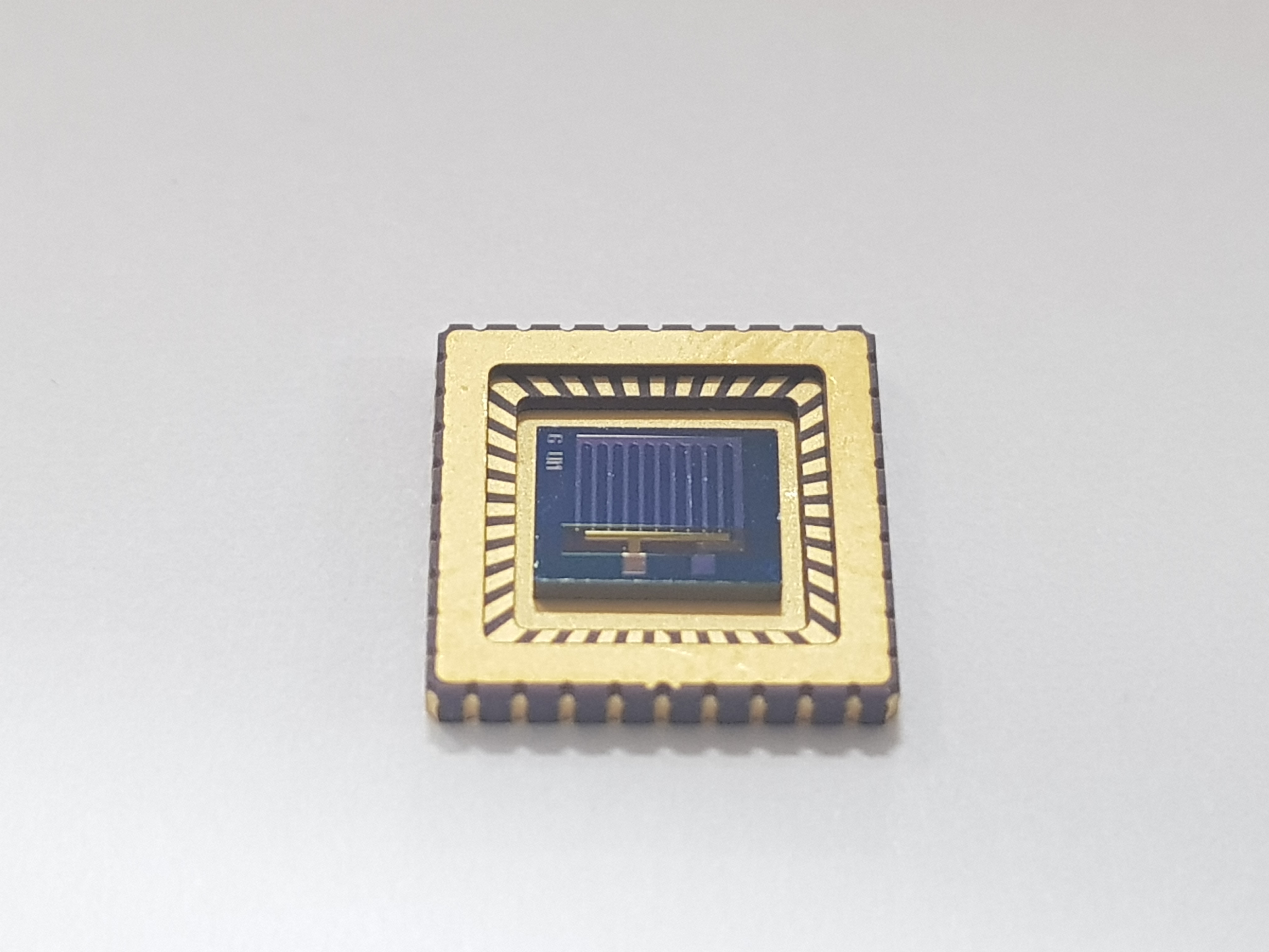 |
Chip on Board (COB)The die is bonded directly to a substrate or a circuit board eliminating the time and cost to mount the die in a package first. The attached and wire bonded die needs to be protected with encapsulation. It is commonly used for LED manufacture, automotive and low cost electronics production. It is also used in aerospace where weight of the packaging is also a concern. | 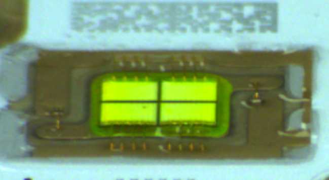 |
3D Integration with Stacked Dies:The die is attached directly to another die or a series of dies to create stacked structures. Stacked structures reduce the amount of space the chips occupy and allow more electronic functionality to be included in a limited space. | 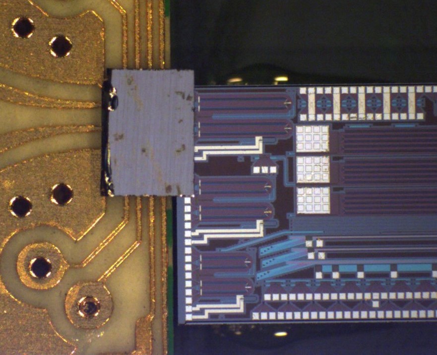 |
System/Package in Package (SiP/PiP)More than one die or discrete component is placed into the same package to allow multiple components to form a sub-system within a single package. | 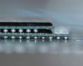 |